- 您现在的位置:买卖IC网 > Sheet目录1992 > CY28551LFXC-3T (Silicon Laboratories Inc)IC CLOCK INTEL/AMD SIS VIA 56QFN
CY28551-3
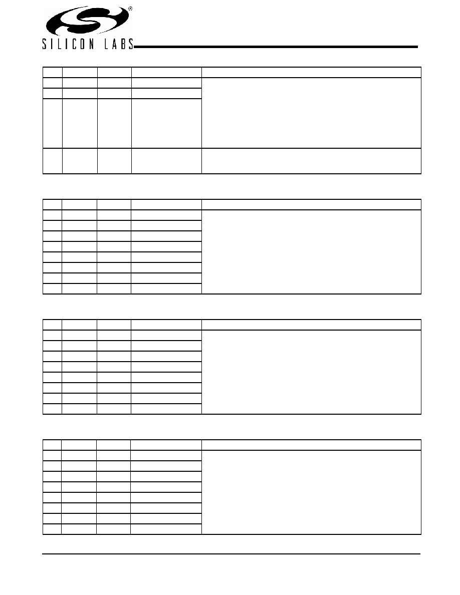
.................... Document #: 001-05677 Rev. *D Page 11 of 28
3
0
R/W
WD_TIMER2
Watchdog timer time stamp selection
000: Reserved (test mode)
001: 1 * Time_Scale
010: 2 * Time_Scale
011: 3 * Time_Scale
100: 4 * Time_Scale
101: 5 * Time_Scale
110: 6 * Time_Scale
111: 7 * Time_Scale
2
0
R/W
WD_TIMER1
1
0
R/W
WD_TIMER0
0
R/W
WD_EN
Watchdog timer enable, when the bit is asserted, Watchdog timer is
triggered and time stamp of WD_Timer is loaded
0 = Disable, 1 = Enable
Byte 13: Control Register 13 (continued)
Bit
@Pup
Type
Name
Description
Byte 14: Control Register 14
Bit
@Pup
Type
Name
Description
7
0
R/W
CPU_DAF_N7
If Prog_CPU_EN is set, the values programmed in CPU_DAF_N[8:0] and
CPU_DAF_M[6:0] will be used to determine the CPU output frequency.
The setting of the FS_Override bit determines the frequency ratio for CPU
and other output clocks. When it is cleared, the same frequency ratio
stated in the Latched FS[E:A] register will be used. When it is set, the
frequency ratio stated in the FSEL[3:0] register will be used.
6
0
R/W
CPU_DAF_N6
5
0
R/W
CPU_DAF_N5
4
0
R/W
CPU_DAF_N4
3
0
R/W
CPU_DAF_N3
2
0
R/W
CPU_DAF_N2
1
0
R/W
CPU_DAF_N1
0
R/W
CPU_DAF_N0
Byte 15: Control Register 15
Bit
@Pup
Type
Name
Description
7
0
R/W
CPU_DAF_N8
If Prog_CPU_EN is set, the values programmed in CPU_DAF_N[8:0] and
CPU_DAF_M[6:0] will be used to determine the CPU output frequency.
The setting of the FS_Override bit determines the frequency ratio for CPU
and other output clocks. When it is cleared, the same frequency ratio
stated in the Latched FS[E:A] register will be used. When it is set, the
frequency ratio stated in the FSEL[3:0] register will be used.
6
0
R/W
CPU_DAF_M6
5
0
R/W
CPU_DAF_M5
4
0
R/W
CPU_DAF_M4
3
0
R/W
CPU_DAF_M3
2
0
R/W
CPU_DAF_M2
1
0
R/W
CPU_DAF_M1
0
R/W
CPU_DAF_M0
Byte 16: Control Register 16
Bit
@Pup
Type
Name
Description
7
0
R/W
PCIE_DAF_N7
The PCIE_DAF_N[8:0] will be used to configure PCIE frequency for Dial-A
Frequency
6
0
R/W
PCIE_DAF_N6
5
0
R/W
PCIE_DAF_N5
4
0
R/W
PCIE_DAF_N4
3
0
R/W
PCIE_DAF_N3
2
0
R/W
PCIE_DAF_N2
1
0
R/W
PCIE_DAF_N1
0
R/W
PCIE_DAF_N0
发布紧急采购,3分钟左右您将得到回复。
相关PDF资料
CY28551LFXC
IC CLOCK INTEL/AMD SIS VIA 64QFN
CY2SSTV855ZXI
IC CLOCK DIFFDRV PLL DDR 28TSSOP
CY2SSTV857ZXI-27
IC CLK DDR266/333BUF1:10 48TSSOP
CY2SSTV857ZXI-32
IC CLK DDR266/333BUF1:10 48TSSOP
CY505YC64DT
IC CLK CK505 BROADWATER 64TSSOP
CYW150OXC
IC CLOCK 440BX AGP 56SSOP
CYW173SXC
IC CLK GEN TAPE DRV 4CH 16SOIC
CYW305OXC
IC CLOCK W305 SOLANO 56SSOP
相关代理商/技术参数
CY28551LFXCT
功能描述:时钟发生器及支持产品 Universal System Clk Intel AMD SiS Via RoHS:否 制造商:Silicon Labs 类型:Clock Generators 最大输入频率:14.318 MHz 最大输出频率:166 MHz 输出端数量:16 占空比 - 最大:55 % 工作电源电压:3.3 V 工作电源电流:1 mA 最大工作温度:+ 85 C 安装风格:SMD/SMT 封装 / 箱体:QFN-56
CY2862-000
制造商:TE Connectivity 功能描述:82A0111-4-9-G110
CY2863-000
制造商:TE Connectivity 功能描述:82A0111-8-9-G110 - Bulk
CY28800
制造商:CYPRESS 制造商全称:Cypress Semiconductor 功能描述:100-MHz Differential Buffer for PCI Express and SATA
CY28800OXC
功能描述:时钟缓冲器 PCI Express & Sata Diff Buffer 100MHz RoHS:否 制造商:Texas Instruments 输出端数量:5 最大输入频率:40 MHz 传播延迟(最大值): 电源电压-最大:3.45 V 电源电压-最小:2.375 V 最大功率耗散: 最大工作温度:+ 85 C 最小工作温度:- 40 C 封装 / 箱体:LLP-24 封装:Reel
CY28800OXCT
功能描述:时钟缓冲器 PCI Express & Sata Diff Buffer 100MHz RoHS:否 制造商:Texas Instruments 输出端数量:5 最大输入频率:40 MHz 传播延迟(最大值): 电源电压-最大:3.45 V 电源电压-最小:2.375 V 最大功率耗散: 最大工作温度:+ 85 C 最小工作温度:- 40 C 封装 / 箱体:LLP-24 封装:Reel
CY28800OXI
功能描述:时钟缓冲器 PCI Express & Sata Diff Buffer 100MHz RoHS:否 制造商:Texas Instruments 输出端数量:5 最大输入频率:40 MHz 传播延迟(最大值): 电源电压-最大:3.45 V 电源电压-最小:2.375 V 最大功率耗散: 最大工作温度:+ 85 C 最小工作温度:- 40 C 封装 / 箱体:LLP-24 封装:Reel
CY28800OXIT
功能描述:时钟缓冲器 PCI Express & Sata Diff Buffer 100MHz RoHS:否 制造商:Texas Instruments 输出端数量:5 最大输入频率:40 MHz 传播延迟(最大值): 电源电压-最大:3.45 V 电源电压-最小:2.375 V 最大功率耗散: 最大工作温度:+ 85 C 最小工作温度:- 40 C 封装 / 箱体:LLP-24 封装:Reel